Blab Tech
TSMC Expands Advanced Packaging in Chiayi to Alleviate AI Chip Bottleneck
Taiwan Semiconductor Manufacturing Company (TSMC) has announced a bold expansion of its advanced packaging capabilities in the Chiayi Science Park, a move that could ease the growing bottleneck in the artificial‑intelligence (AI) chip supply chain.
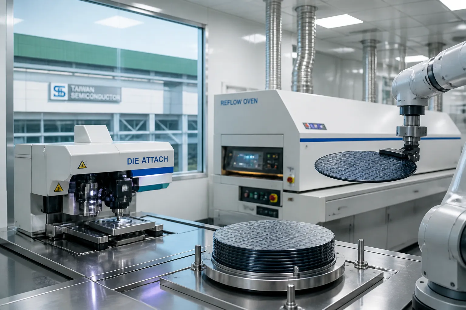
During a groundbreaking ceremony on Sunday, National Science and Technology Council minister Wu Cheng‑wen unveiled plans for three new packaging facilities that will cover roughly 90 hectares of the park’s second phase. The sites will form a dedicated cluster led by TSMC, with two plants already in mass‑production as of June. Once both phases are fully operational, the complex is projected to generate more than NT$300 billion (US$9.35 billion) in annual output and support about 9,000 jobs.
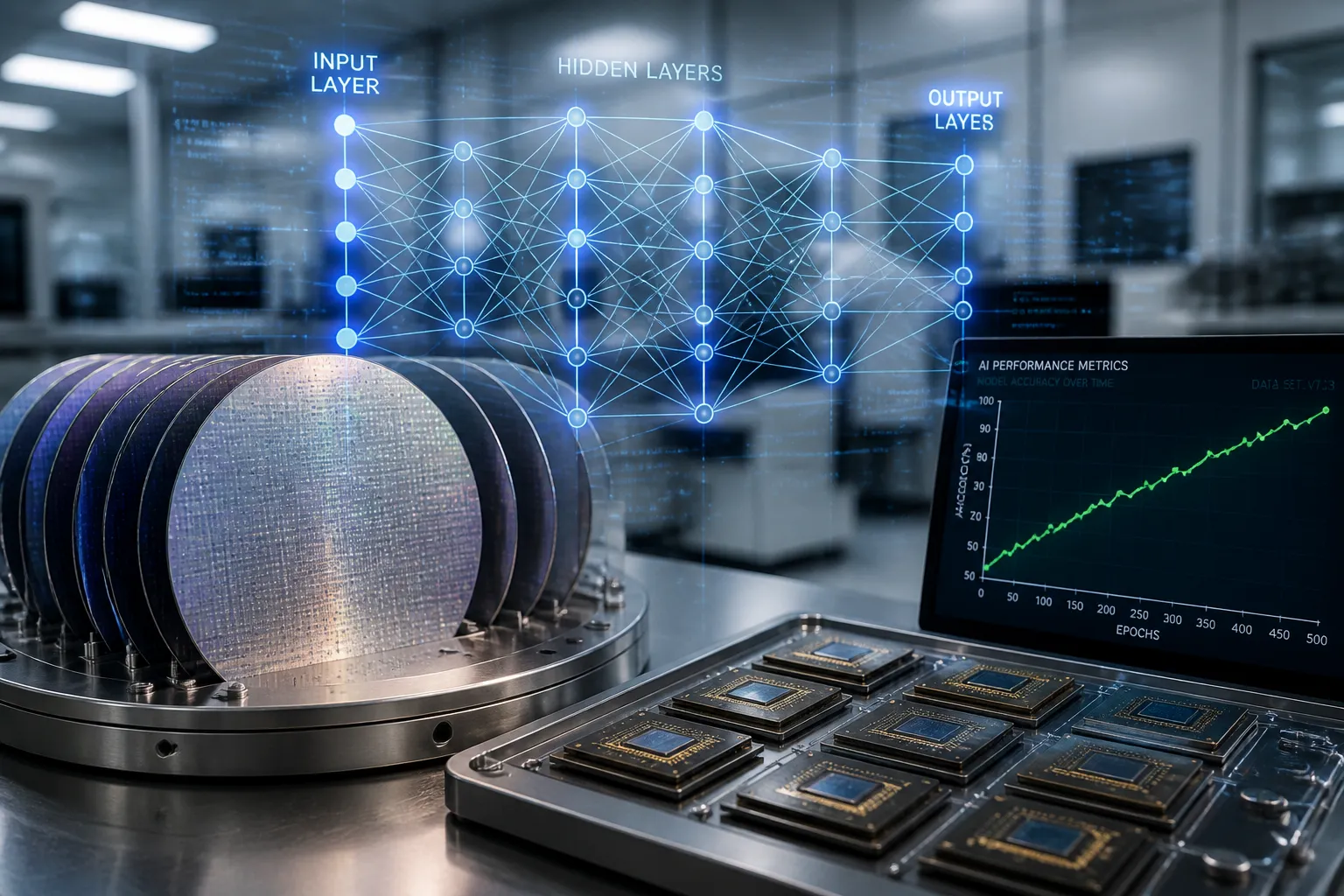
Advanced packaging—specifically the Chip‑on‑Wafer‑on‑Substrate (CoWoS) technology—combines logic dies with high‑bandwidth memory (HBM) into a single package. Over the past two years, CoWoS has been the limiting factor for AI accelerators from every major vendor, including Nvidia and Google. Nvidia’s multi‑year HBM4 deal with SK Hynix, for instance, was designed to relieve the same constraint.
Wu emphasized that the Chiayi site will link with other science parks in southern Taiwan—Tainan, Kaohsiung, and Pingtung—as well as the Central Taiwan and Hsinchu parks, creating what he called the world’s most comprehensive AI and semiconductor corridor. He also noted that biotechnology, aerospace, and precision‑machinery firms are expected to join the ecosystem over time.
The announcement arrived as TSMC reported record second‑quarter revenue of T$1.27 trillion (US$39.62 billion), up 36 % year‑on‑year and slightly ahead of an LSEG SmartEstimate drawn from 20 analysts. June revenue alone rose 67.9 % from a year earlier to T$442.68 billion. The company gave no forward guidance in the statement and will update its outlook at its earnings conference on Thursday, where analysts expect a 58.8 % rise in second‑quarter net profit.
TSMC’s Taipei‑listed shares closed up 1 % on Monday, while the broader market finished flat. The company is now Asia’s most valuable listed business, with a market capitalisation of about US$1.96 trillion, and its shares have risen 57 % this year.
Despite the scale of the expansion, Wu did not provide a construction timeline, a cost estimate for the Phase II fabs, or a date for when the new capacity will come online. TSMC has not issued a separate statement on the project, and the figures so far come from the government.
Chiayi County, historically an agricultural region, is now being asked to host the packaging step that determines how many AI accelerators the world will ship. The move reflects the broader trend of Taiwan’s semiconductor ecosystem shifting from pure fabrication to advanced packaging, a shift that has been driven by the rapid growth of AI workloads.
The expansion is part of a larger strategy to meet the rising demand for high‑performance computing chips. Advanced packaging allows multiple devices—such as processors and memory—to be merged into a single package, reducing signal path length and improving performance without requiring further node shrinkage. This capability is critical as AI models grow larger and more memory‑intensive.
The industry has seen a shift in bottlenecks: while the past global chip shortage was largely driven by pandemic‑related disruptions, the current shortage is largely a result of reallocating manufacturing capacity toward AI data‑center products. This has compressed commodity DRAM supply and increased prices for high‑bandwidth memory.
In summary, TSMC’s planned expansion in Chiayi is a significant step toward addressing the packaging bottleneck that limits AI accelerator production. The project’s completion timeline and cost remain unclear, but the move is expected to strengthen Taiwan’s position as a global hub for advanced semiconductor manufacturing.
During a groundbreaking ceremony on Sunday, National Science and Technology Council minister Wu Cheng‑wen unveiled plans for three new packaging facilities that will cover roughly 90 hectares of the park’s second phase. The sites will form a dedicated cluster led by TSMC, with two plants already in mass‑production as of June. Once both phases are fully operational, the complex is projected to generate more than NT$300 billion (US$9.35 billion) in annual output and support about 9,000 jobs.
Advanced packaging—specifically the Chip‑on‑Wafer‑on‑Substrate (CoWoS) technology—combines logic dies with high‑bandwidth memory (HBM) into a single package. Over the past two years, CoWoS has been the limiting factor for AI accelerators from every major vendor, including Nvidia and Google. Nvidia’s multi‑year HBM4 deal with SK Hynix, for instance, was designed to relieve the same constraint.
Wu emphasized that the Chiayi site will link with other science parks in southern Taiwan—Tainan, Kaohsiung, and Pingtung—as well as the Central Taiwan and Hsinchu parks, creating what he called the world’s most comprehensive AI and semiconductor corridor. He also noted that biotechnology, aerospace, and precision‑machinery firms are expected to join the ecosystem over time.
The announcement arrived as TSMC reported record second‑quarter revenue of T$1.27 trillion (US$39.62 billion), up 36 % year‑on‑year and slightly ahead of an LSEG SmartEstimate drawn from 20 analysts. June revenue alone rose 67.9 % from a year earlier to T$442.68 billion. The company gave no forward guidance in the statement and will update its outlook at its earnings conference on Thursday, where analysts expect a 58.8 % rise in second‑quarter net profit.
TSMC’s Taipei‑listed shares closed up 1 % on Monday, while the broader market finished flat. The company is now Asia’s most valuable listed business, with a market capitalisation of about US$1.96 trillion, and its shares have risen 57 % this year.
Despite the scale of the expansion, Wu did not provide a construction timeline, a cost estimate for the Phase II fabs, or a date for when the new capacity will come online. TSMC has not issued a separate statement on the project, and the figures so far come from the government.
Chiayi County, historically an agricultural region, is now being asked to host the packaging step that determines how many AI accelerators the world will ship. The move reflects the broader trend of Taiwan’s semiconductor ecosystem shifting from pure fabrication to advanced packaging, a shift that has been driven by the rapid growth of AI workloads.
The expansion is part of a larger strategy to meet the rising demand for high‑performance computing chips. Advanced packaging allows multiple devices—such as processors and memory—to be merged into a single package, reducing signal path length and improving performance without requiring further node shrinkage. This capability is critical as AI models grow larger and more memory‑intensive.
The industry has seen a shift in bottlenecks: while the past global chip shortage was largely driven by pandemic‑related disruptions, the current shortage is largely a result of reallocating manufacturing capacity toward AI data‑center products. This has compressed commodity DRAM supply and increased prices for high‑bandwidth memory.
In summary, TSMC’s planned expansion in Chiayi is a significant step toward addressing the packaging bottleneck that limits AI accelerator production. The project’s completion timeline and cost remain unclear, but the move is expected to strengthen Taiwan’s position as a global hub for advanced semiconductor manufacturing.