Blab Tech
TSMC Develops EMIB-Like Packaging to Match Intels Advanced Chip Technology
In a bid to keep pace with Intel’s high‑bandwidth chiplets, TSMC is quietly forging a new packaging path that mirrors the company’s own Embedded Multi‑Die Interconnect Bridge (EMIB). The Information reports that the Taiwan semiconductor foundry is partnering with Kinsus Interconnect Technology Corp., a local supplier of substrates and interposer materials, to build what it calls an "EMIB‑like" solution.
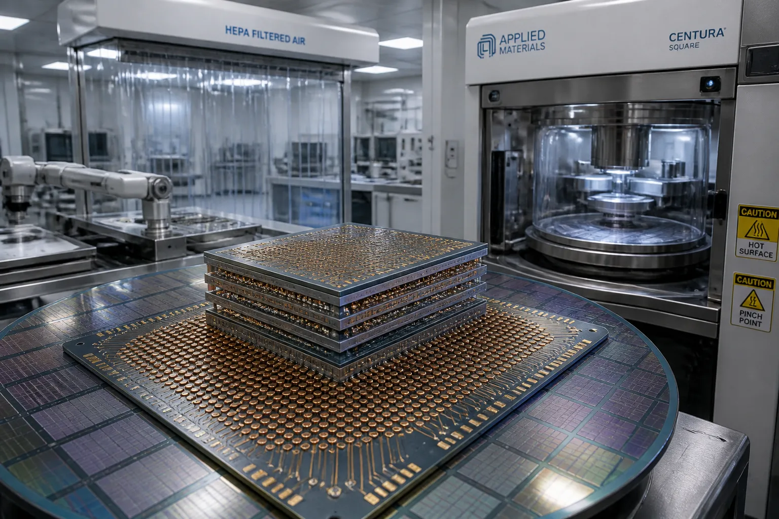
Intel’s EMIB is a 2.5‑D packaging technology that places multiple dies side‑by‑side on a silicon interposer, enabling high‑bandwidth links without the need for through‑silicon vias (TSVs). The chip is already in use in Intel’s Sapphire Rapids server processors and in a range of external products sold through Intel Foundry Services. By contrast, TSMC’s most widely used advanced packaging platform is CoWoS (Chip‑on‑Wafer‑on‑Substrate), which stacks dies vertically and relies on TSVs for inter‑die communication.
During its earnings call in early July, TSMC CEO Che‑Chia Wei said the company’s current advanced‑packaging capacity was a bottleneck for customers. "Our advanced‑packaging technology is limiting customers’ growth due to its capacity constraints," Wei said. The remark came amid a surge in demand for AI accelerators and high‑performance computing chips, many of which rely on chiplet architectures that require sophisticated packaging.
The move toward an EMIB‑style interposer is seen as a response to the need for higher bandwidth and lower latency between chiplets. While CoWoS can deliver dense interconnects, the TSV process it relies on limits the number of wafers that can be processed each month. An EMIB‑like interposer, which eliminates the redistribution layer and TSVs, could offer a simpler, more scalable route to multi‑die integration.
Kinsus Interconnect Technology Corp. has long produced ball‑grid‑array (BGA) substrates and other interposer materials for the semiconductor industry. Its expertise in fine‑pitch interconnects and substrate engineering makes it a natural partner for TSMC’s packaging research. The Information report did not disclose technical details of the collaboration, but it noted that the partnership focuses on developing a stack that can match Intel’s EMIB performance while leveraging TSMC’s existing manufacturing infrastructure.
Industry analysts view the development as part of a broader trend in which foundries expand their packaging portfolios to serve AI and high‑performance computing customers. Advanced packaging has become a key differentiator because it allows designers to mix and match dies from different process nodes and manufacturers. As AI workloads grow, the demand for high‑bandwidth, low‑power interconnects is expected to rise.
At present, no public launch date has been announced for TSMC’s EMIB‑like technology. The company has said it remains in the research and development phase, and that any commercial deployment would follow a rigorous validation process. Meanwhile, TSMC continues to invest heavily in expanding its CoWoS capacity, targeting a 50% increase in wafer starts by 2027.
In short, TSMC’s collaboration with Kinsus Interconnect Technology Corp. to develop an EMIB‑like packaging solution reflects the foundry’s effort to address capacity constraints and to offer customers a high‑performance, scalable alternative to its existing CoWoS platform. The initiative underscores the importance of advanced packaging in the semiconductor supply chain, particularly for AI and high‑performance computing applications, and the industry will be watching closely for further technical details and the eventual commercial rollout of the new packaging technology.
Intel’s EMIB is a 2.5‑D packaging technology that places multiple dies side‑by‑side on a silicon interposer, enabling high‑bandwidth links without the need for through‑silicon vias (TSVs). The chip is already in use in Intel’s Sapphire Rapids server processors and in a range of external products sold through Intel Foundry Services. By contrast, TSMC’s most widely used advanced packaging platform is CoWoS (Chip‑on‑Wafer‑on‑Substrate), which stacks dies vertically and relies on TSVs for inter‑die communication.
During its earnings call in early July, TSMC CEO Che‑Chia Wei said the company’s current advanced‑packaging capacity was a bottleneck for customers. "Our advanced‑packaging technology is limiting customers’ growth due to its capacity constraints," Wei said. The remark came amid a surge in demand for AI accelerators and high‑performance computing chips, many of which rely on chiplet architectures that require sophisticated packaging.
The move toward an EMIB‑style interposer is seen as a response to the need for higher bandwidth and lower latency between chiplets. While CoWoS can deliver dense interconnects, the TSV process it relies on limits the number of wafers that can be processed each month. An EMIB‑like interposer, which eliminates the redistribution layer and TSVs, could offer a simpler, more scalable route to multi‑die integration.
Kinsus Interconnect Technology Corp. has long produced ball‑grid‑array (BGA) substrates and other interposer materials for the semiconductor industry. Its expertise in fine‑pitch interconnects and substrate engineering makes it a natural partner for TSMC’s packaging research. The Information report did not disclose technical details of the collaboration, but it noted that the partnership focuses on developing a stack that can match Intel’s EMIB performance while leveraging TSMC’s existing manufacturing infrastructure.
Industry analysts view the development as part of a broader trend in which foundries expand their packaging portfolios to serve AI and high‑performance computing customers. Advanced packaging has become a key differentiator because it allows designers to mix and match dies from different process nodes and manufacturers. As AI workloads grow, the demand for high‑bandwidth, low‑power interconnects is expected to rise.
At present, no public launch date has been announced for TSMC’s EMIB‑like technology. The company has said it remains in the research and development phase, and that any commercial deployment would follow a rigorous validation process. Meanwhile, TSMC continues to invest heavily in expanding its CoWoS capacity, targeting a 50% increase in wafer starts by 2027.
In short, TSMC’s collaboration with Kinsus Interconnect Technology Corp. to develop an EMIB‑like packaging solution reflects the foundry’s effort to address capacity constraints and to offer customers a high‑performance, scalable alternative to its existing CoWoS platform. The initiative underscores the importance of advanced packaging in the semiconductor supply chain, particularly for AI and high‑performance computing applications, and the industry will be watching closely for further technical details and the eventual commercial rollout of the new packaging technology.